Professor De Boer's list of
TEXTBOOK ERRATA
(last update 8/27/2020)

Sedra & Smith,
Microelectronic Circuits, 7th Ed.
ISBN 978-0-19933913-6
Oxford, 2015.
Link to errata for the 5th edition, 6th edition, 8th edition.
If you are considering purchasing this textbook but are worried that it is a poor choice due to this list of known errata, please don't worry about that. Competing textbooks have about as many errata, but perhaps no list like this. "Better the devil you know than the devil you don't know." Professor De Boer likes this book enough to find it worthwhile to publish this list of errata.
This list is in addition to the publisher's list of errata.
This list was prepared from the first printing of the textbook.
Some of these errata may be corrected in later printings. Some additional errata could accidentally be introduced into later printings! Where I have information on errata unique to later printings, there are appropriate annotations.
Page 45, Problem 1.7
Replace the problem statement with this:
1.7 The voltage divider shown in Figure
P1.6(a) has R1 = 3-kΩ and
R2 = 2-kΩ. A 5 V
ground-referenced power supply is connected to
VDD.
The output, VO is intended to be 2 V.
a.) Assuming exact-valued resistors, what
output voltage with
respect to ground actually results?
b.) Assuming exact-valued resistors, what
equivalent output
resistance results?
c.) If the resistors are not ideal but have a ±5%
manufacturing tolerance, what are the extreme output
voltages
and output resistances that can result?
(Posted 8/19/2016)
Page 74, Equation 2.9
The ratio of resistances is the reciprocal of what it should
be. The correct equation is:
![]()
(Posted 9/13/2016)
Pages 90-92, All integrals
An example of this errata is found in Equation 2.25 on page 90.
The integral has an upper limit of t, but it also
uses the symbol t as the variable of integration.
The limit and the variable of integration cannot be
one-and-the-same. Change the variable of integration to λ.
A corrected version of Equation 2.25 is
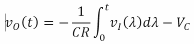
Similar corrections are needed in five more instances as follows:
Page 90, four lines from the top, two inline expressions
Page 90, sixth line down, the displayed equation for vC(t)
Page 91, inside Figure 2.24(a), the displayed equation for vO(t)
Page 92, the integral near the middle of the blue display box of Example 2.5
(Posted 9/15/2018)
Page 121, Problem D2.34 part (d)
Add the word "Norton" so that part (d) reads as follows:
(d) If the amplifier is fed with a Norton current source
having a
current of 0.2 mA and a source resistance of
10 k , find
iL.
, find
iL.
Also see below for a clarification of Part (b).
(Posted 8/12/2016)
Page 130, Problem D2.92
In the the problem statement two instances of the phrase,
"3-dB frequency" should be, "–3-dB frequency."
Alternatively, add the word, "down" so that the
phrase reads, "3 dB down frequency."
(Posted 9/19/2018, updated 8/27/2020)
Page 234, Problem 4.22 part (d)
Delete part (d) from the problem.
(It is a duplicate of Part(b))
(Posted 8/12/2016)
Page 240, Problem 4.66 parts (c, d)
In part (c) add the phrase, "of the nominal output voltage" so
that the second sentence of part (c) reads, "What is the change
in VO expressed as a percentage of the
nominal output voltage, corresponding to the ±25%
change in VS?"
In part (d), again add the phrase, "of the nominal output
voltage" so that the second sentence of part (d) reads,
"By what percentage of the nominal output voltage does
VO change from the no-load to the full-load
condition?"
(Posted 9/25/2018)
Page 241, Problem 4.77 part (c)
Add, "during conduction" to part (c) so that it reads,
"(c) What is the average diode current during conduction?"
(Posted 8/17/2016)
Page 241, Problem 4.78.
In part (b) of the statement from problem 4.77, add the word
"each" before the word "diode." The problem then reads
(b) For what fraction of the cycle is there condition through
each diode?
In part (c) delete the existing word "diode" and append the
phrase, "through each diode during conduction."
The question then reads. . .
(c) What is the average current through each diode
during conduction?
In part (d) add the phrase, "through each diode?" and delete
one instance of the word "diode." The question
then reads. . .
(d) What is the peak current through each diode?
Also see below for a clarification of
this problem.
(Posted 8/17/2016, updated 9/26/2016)
Page 241, Problem 4.79.
In part (b) of the statement from problem 4.77, replace the
phrase, "does the diode conduct" with the phrase, "is there
conduction through the secondary winding of the transformer."
The problem then reads
(b) For what fraction of a cycle is there conduction through the
secondary winding of the transformer?
In part (c) add the phrase, "through each diode during
conduction." and delete one instance of the word "diode."
The question then reads. . .
(c) What is the average current through each diode during conduction?
In part (d) add the phrase, "through each diode?" and delete
one instance of the word "diode." The question then reads. . .
(d) What is the peak current through each diode?
Also see below for a clarification of this
problem.
(Posted 8/17/2016)
Page 264, Line just above Section 5.2.
Replace "Chapter 14" with "Chapter 15, Section 15.1.4"
(Posted 10/17/2018)
Page 292, Problem D5.5
Change the last line of the problem statement from,
"maximum allowed voltage of 1.8 V." to,
"maximum allowed VGS of 1.8 V."
(Posted 8/17/2016)
Page 295, Problem 5.24
In the problem statement replace "(a)" with "(i)" and
replace "(b)" with "(ii)." Leave the "(a)" and "(b)" in
Figure P5.24 as they are. There are two parts to the problem,
part (i) and part (ii) and each of those parts needs to be
considered once for (a) the n-channel MOSFET and once for (b)
the p-channel MOSFET, a total of four things to consider.
(Posted 8/17/2016.)
Page 297, Problem 5.31
Add "in saturation" near the end of the first line of the
problem statement so that the first line becomes,
"A particular MOSFET has VA = 20 V.
For operation in saturation at"
(Posted 8/17/2016.)
Page 373, Figure 7.4(b)--Incorrectly shaped slope between Q and B.
The artist's inclusion of an inflection in the slope of the
curve between Q and B is wrong. Point A is the vertex of a
downward-opening parabola. The curve between points A and B
is entirely parabolic, as described by Equation 7.5 on page
370. The slope continues to become monotonically more negative
going along the arc from A, through Q, to B. The curve from
point C to point B meets that arc tangentially at point B so
that there is no discontinuity in the slope of the curve.
Figure 7.3(b) shows these details correctly. (This same
error appears in the 8th edition on page 371.)
(Posted 4/25/2020
— Thanks to Dylan Gulledge of The University of Northern
Texas for pointing this out.)
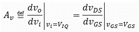
Page 374, Equation 7.13
The equation given is not the definition of
Av.
Change equation 7.13 to read as follows:
Page 480, Problem 7.5 part (c)
Replace the phrase, "and disregarding the distortion caused by the MOSFET's square-law characteristic," with the phrase, "and by using equations valid for large signals," . . .
The printed phrase is ambiguous. It has at least two equally valid interpretations. First, as the author intended, "disregard" meaning, "do not use a small-signal approximation to eliminate the distortion from the calculation, instead allow the distortion to be included in the calculation. Second, "disregard" meaning assume a linear approximation as if no distortion existed.Page 485, Problem 7.30.
(Posted 12/08/2016)
Replace the first sentence with: "Model the NMOS amplifier shown in Fig. P7.30 using a T equivalent circuit, assuming λ = 0."
("Replace the transistor. . ." misleads students into thinking that the DC sources, VDD and VSS play a part in the solution. In the needed small-signal analysis those DC sources get set to zero or ground.) (Posted 8/17/2016)Page 489, Problem D7.58.
Be sure to look at the text below Figure P7.58. The problem statement continues there.
The layout on the page of Figure P7.58 confusingly interrupts the problem statement. Figure P7.58 should be moved down below the end of the problem statement and just above the heading "Section 7.3: Basic Configurations." (Posted 11/27/2016)Page 489, Problem D7.60 Part (a).
Change, "signal strength" to "signal voltage."
(Posted 8/17/2018)
Page 497, Problem 7.118 Part (a).
Change, part (a) of the problem statement to:
(a) Neglecting Early effect, if the MOSFET is operating
in saturation with ID = 0.5 mA and Vov = 0.3 V,
what must the MOSFET's kn be? What is the DC
voltage at the drain?
The one cannot "verify" the operating point without first knowing kn.Page 498, Problem 7.120.
The author intends for kn to be "found." (Posted 12/05/2018)
Add this sentence to the problem statement:
"Assume the transistors have identical specifications."
Also see the additional note on this problem. (Posted 8/16/2016)
Page 576, Problem 8.3.
Insert a sentence so that the end of the problem statement reads as:
". . . high as 1.1 V. Choose the ratio W/L to maximize the magnitude of the overdrive voltage at the diode-connected transistor. Also neglect channel-length modulation." (Posted 1/25/2019)
Page 580, Problem 8.26.
Add, "for both bias levels." to the last line of the problem statement so that the last line reads:
"vo/vsig, for both bias levels." (Posted 8/17/2016)
Page 588, Problem 8.78.
In the equation for Av change the "equals" sign (=) to an "approximately equal" (≈) sign. (Posted 8/17/2016)
Pages 632, 633, Example 9.4.
There is no errata in the textbook on these pages, but. . .
The publisher's errata on these pages is itself errata.
Ignore the publisher's errata on pages 632 and 633.
Here is a more complete version of Example 9.4. (Posted 3/16/2019)
Page 707, Equation 10.13.
There is a problem with units. The reciprocal of an RC time constant yields units of radians/second. The variable f implies the units of Hertz.
Equation 10.13 should either be

or

(Posted 3/06/2019)
Page 768, Figure 10.34 (a).
At the drain of QS (the blue text) change ZSS = RSS||CSS to ZSS = RSS||ZCSS
The operator colloquially called "in parallel with" can be interpreted as a mathematical operator. To wit,Page 800, Problem 10.80, last line of the problem statement
a||b = 1/[(1/a) + (1/b)]
In other words, || can mean, "take the reciprocal of the sum of the reciprocals." Given this interpretation, the expression RSS||CSS has a mis-match of units. Expressing this concept in terms of impedances is more correct.
The use of the || symbol as a mathematical operator, rather than simply as a substitute for the phrase, "in parallel with" is well entrenched in electrical engineering literature but is not formally standardized as far as Prof. dDB knows. This can lead to real confusion. For example, in the expression
Ceq = C1||C2 does this mean that the capacitors are, "in parallel" and thus the equivalent capacity is a sum, or does it mean that the capacitors are in series and the equivalent capacity is, "the reciprocal of the sum of the reciprocals?" This confusion can be avoided by using the parallel symbol, ||, only with impeadances, e.g. Zeq = ZC1||ZC2. Then the symbol means the same thing no matter which way it is interpreted.
Reference: Wikipedia talk page on "Parallel (operator)"
https://en.wikipedia.org/wiki/Talk:Parallel_(operator) (Posted 4/10/2019)
(More easiliy noticed as the line just above Problem 10.81.)
If your printing of the textbook shows the line as,
gm = 5 ma/V, Cgd = 10 pF, and Cgs = 2 pF.
then swap the capacitor values around.
The correct line is:
gm = 5 ma/V, Cgd = 2 pF, and Cgs = 10 pF.
This error has been fixed in later printings. The corrected line is consistent with the answer given in the instructor's solution manual. It also, "just makes sense," because usually Cgd < Cgs. (Posted 4/10/2019)Page 801, Problem 10.96, second line of the problem statement
Replace "ggd = 0.01 pF" with "Cgd = 0.01 pF"
(Posted 4/23/2019)
Pages 817 and 818, Bottom half of the page
The discussion of signal-to-interference ratio presented (as printed) is in terms of a voltage ratio. This is not a common practice in the industry. Usually the signal-to-interference ratio is defined as a power ratio. More generally, the signal-to-interference ratio is a special type of signal-to-noise ratio, which is also a power ratio. The following changes make the text conform to industry standard practice.
Change the second line under heading 11.2.3 by
adding the word "power" in two places so that the line reads:
". . .precisely, to increase the ratio of signal power to interference power. However. . ."
Change the line just above Equation 11.15 by
adding the word "power" so that the line reads:
"amplifier. The signal-to-interference power-ratio for this amplifier is"
Change Equation 11.15 to S/I = Vs2/Vn2
Change the line above Equation 11.17 by
adding the word "power" so that the line reads:
"Thus the signal-to-interference power-ratio at the output becomes"
Change Equation 11.17 to
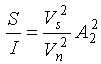
In the line below Equation 11.17 change, "which is A2 times higher" to,
"which is A22 times higher".
References:Appendix L, Page L-4, Answer to Problem 4.9(a).
—The definition of signal-to-noise ratio as a power ratio (not a voltage ratio) can be found in most handbooks of electrical engineering and also in. . .
—B.P. Lathi, Linear Systems and Signals, 2nd ed. Oxford, 2005, p70.
—Pallas-Areny and Webster, Analog Signal Processing, Wiley-Interscience, 1999, page 16 and pages 525-526.
—Millman and Halkias, Integrated Electronics: Analog and Digital Circuits and Systems, McGraw Hill, 1972, p403.
—Horowitz and Hill, The Art of Electronics, 2nd edition, Cambridge, 1989, p434.
— Hambley, Electronics: A Top-Down Approach to Computer-Aided Circuit Design, Macmillan, 1994, p382.
—The definition of signal-to-interferance ratio as a power ratio and as a special case of a signal-to-noise ratio can be found in the Wikipedia article "Signal-to-interference ratio."
—A discussion of Signal to Noise ratio as a power ratio can be found in the Wikipedia article , "Signal-to-noise ratio."
A few other authors along with Sedra and Smith treat signal-to-noise ratio (or signal to interference ratio) as a voltage ratio (not a power ratio), nevertheless, it does not agree with industry practice. Some examples are:
—Gray and Searle, Electronic Principles: Physics, Models, and Circuits, Wiley, 1969, p622. (This is the earliest published book Prof. De Boer could find with this error in it.)
—Donald Neamen, Microelectronics Circuit Analysis and Design, 4th ed., McGraw Hill, 2010, p859.
(Posted 8/17/2016)
In the answer for Problem 4.9 part (a), change "V = 1 V;" to
"V = –1 V;" (Posted 9/22/2018)
Appendix L, Page L-5, Answer to Problem 4.66.
There are errors of precision and other errors in the answers given.
Correct answers are:
(a) 9.825 V; (b) 205.6 Ω; (c) 3.293%, 3.293% of 10 V; (d) –6.770 Ω, –1.354% of 10 V; (e) 71.38 mA, 0.7370 W
(Posted 9/25/2018)
Appendix L, Page L-5, Answer to Problem 5.1.
Replace "580 to 2900 μm2"
with "58 to 290 μm2" (Posted 10/19/2018)
Appendix L, Page L-7, Answer to Problem 6.58.
There are rounding errors. Assuming |VBE| = 0.7 V, more accurate answers are +0.42 V, +1.12 V, –1.16 V; +1.2 V, +1.9 V, –1.9 V, 206
(Posted 11/07/2018, updated 11/08/2018)
Appendix L, Page L-7, Answer to Problem 6.63.
The answers given do not meet the specifications of the problem statement. With a little calculation it is clear that the emitter current will be out-of-specification for the β = 50 case. Correct answers are:
RB = 30 kΩ, RC = 4 kΩ, RE = 4 kΩ,
(0.919 mA) ≤ IC ≤ (1.004 mA) and (–1.33 V) ≤ VC ≤ (–0.903 V)
Hint: It is not sufficient to solve for the three resistor values and then round all three values. The emitter current is particularly sensitive to the value of RE. After that is rounded it will be necessary to recalculate RB to reset the emitter current back to 1 mA for the case of β = 100.
Note: A case might be made for adjusting RB as high as 39 kΩ. All specifications will then be met except that the emitter current for the case of β = 100 will be a bit low. (Posted 11/09/2018)
Appendix L, Page L-9, Answer to Problem 8.1.
The first answer given is wrong and the second is of poor accuracy.
Change 12 kΩ; 0.2 V; 25 kΩ; 20 μA to
7.2 kΩ; 0.18 V; 25 kΩ; 20 μA
Also, if the Early effect is ignored for Q1 only, then the answers are:
7.0 kΩ; 0.2 V; 25 kΩ; 20 μA
(Posted 2/11/2017)
Appendix L, Page L-11, Answer to Problem 8.90 Part (b).
The "0.7 μA" answer given is wrong.
The correct answer is 0.61 μA.
(Posted 2/05/2019)
Appendix L, Page L-13, Answers to Problem 10.3.
The answers given are wrong.
The correct answers are 9 μF, 98.2 Hz, 9.82 Hz.
(Posted 3/12/2019)
Appendix L, Page L-15, Answer to Problem 10.106(b).
The answer given for part (b) is wrong.
The correct answer is 2.66 kHz.
This error also appears in the instructor's solution manual.
(Posted 4/23/2019)
Additional notes: (Clarifications--not errata)
Page 48 Problem 1.25
An equivalent problem (Implying the same questions and giving the same answer) is as follows:
Suppose a temperature sensor is at a temperature of T degrees centigrade. At this temperature and without the load resistance connected, an ideal voltmeter shows the output voltage to be V millivolts. A 5 kΩ load resistance is now connected but the temperature is not changed. The terminal voltage of the sensor is reduced to V – 10 millivolts. Now the temperature is increased until the terminal voltage returns to V millivolts. It is observed that the temperature was increased 10 degrees centigrade to accomplish this. What is the source resistance of the sensor?
(Posted 8/16/2016, updated 9/8/2016)
Page 121 Problem D2.34 part (b)
The output resistance of the "current amplifier" is requested. The variable vo designates the output of the "operational amplifier" which is confusingly, not the output of the "current amplifier." The output of the "current amplifier" is the current, iL through the load resistor, RL.
Hint: Add label VL under RL and polarity marks "+" and "–" on either side with the "+" on the left. Then the output of the "current amplifier" is the load current, iL = VL/RL.
To find the output resistance of the "current amplifier," replace RL by a test source, Vx such that VL = Vx. Then, with the input of the "current amplifier" zeroed (iI = 0 or open) find iL in terms of VL. Then the output resistance is Ro = VL/iL. See text page 29 for the basic theory. Note that for a current amplifier, a zero input is an open. (Whereas, for a voltage amplifier a zero input is a connection to ground.)
Also see above for errata on Part (d). (Posted 8/16/2016)
Page 127. Problem *2.77 and Figure P2.77
Clarification #1
The problem statement continues on page 128. (Posted 9/06/2016)
Clarification #2
The two resistors connected to the non-inverting ("+") inputs of the op-amps are for the purpose of reducing the non-ideal effects of input bias currents to the op-amps. The assumption of an "ideal" op-amp makes these resistors unimportant to the operation of the circuit, no matter what their values are. If the op-amps are ideal these resistors may be set to zero (replaced with wires) without any change to the operation of the circuit. Additionally, although the two 10 k
resistors as
shown will reduce the harmful non-ideal effects of input bias
currents, these resistors are not shown with their optimal values.
For this circuit, the non-inverting input of the top op-amp should
be connected to node A through a
6.67 k resistor. The
non-inverting input of the bottom op-amp should be connected to
ground through a 7.5 k
resistor. These are the Thevenin-equivalent resistances seen by
the inverting inputs of the op-amps. If this makes no sense to
you and you are further interested, ask professor De Boer
about it. (Posted 8/16/2016, updated 9/05/2018)
Page 130. Problem D**2.93
For stylistic consistency, in the denominator of the equation the second instance of j could be inside the parenthesis. The complete denominator is then
[1 + (ω1/jω)][1 + (jω/ω2)]
Either way, the equation means the same thing. (Posted 8/16/2016)Page 204–206 Example 4.7
In the statement of the example problem VZ = 6.8 V at IZ = 5 mA is given. This does not mean that the actual diode current, labeled in blue as "IZ" on the figure, is necessarily 5 mA. It only means that if IZ is 5 mA then VZ will be 6.8 V.
(In the figure, in both parts (a) and (b), VO = VZ. (Posted 8/16/2016)
Page 241 Problem 4.78
Here is the question stated in one piece, with errata corrected:
4.78 Let the full-wave rectifier circuit shown in Figure 4.24 (page 211) operate from a 120 V (rms) 60 Hz residential supply line. Let the transformer have a 6:1 (step down) turns ratio. (The turns ratio from the primary to each half of the secondary is 12:1.) Let the diodes be silicon diodes that can be modeled to have a 0.7 V drop for any forward current. Let the load resistor be 1 kΩ. Augment this rectifier circuit with a capacitor chosen to provide peak-to-peak ripple voltage of
(i) 10% of the peak output and
(ii) 1% of the peak output.
In each of the above cases:
a.) What average output voltage results?
b.) For what fraction of a cycle is there conduction through each diode?
c.) What is the average current through each diode during conduction?
d.) What is the peak current through each diode?
Note: a "rectifier" is a diode or—in this case—a set of diodes used to convert alternating current to direct current.
Also see above for errata on this problem.
(The original problem statement refers to Problems 4.71 and 4.77. Problem 4.77 refers to Problem 4.70. Problem 4.70 refers by name—not by figure number—to Figure 4.23, but students are supposed to substitute Figure 4.24 because problem 4.71 refers to that by name and by way of superseding problem 4.70 because problem 4.78 mentions problem 4.71 instead of Problem 4.70. Even some professors have a hard time understanding the question as presented in the textbook!)
(Posted 8/16/2016)
Page 241 Problem 4.79
Here is the question stated in one piece, with errata corrected:
4.79 Let the full-wave bridge rectifier circuit shown in Figure 4.25 (page 212) operate from a 120 V (rms) 60 Hz residential supply line. Let the transformer have a 12:1 (step down) turns ratio. Let the diodes be silicon diodes that can be modeled to have a 0.7 V drop for any forward current. Let the load resistor be 1 kΩ. Augment this rectifier circuit with a capacitor chosen to provide peak-to-peak ripple voltage of
(i) 10% of the peak output and
(ii) 1% of the peak output.
In each of the above cases:
a.) What average output voltage results?
b.) For what fraction of a cycle is there conduction through the secondary
winding of the transformer?
c.) What is the average current through each diode during conduction?
d.) What is the peak current through each diode?
Also see above for errata on this problem.
(The original problem statement refers to Problems 4.72 and 4.77. Problem 4.77 refers to Problem 4.70. Problem 4.70 refers by name—not by figure number—to Figure 4.23, but students are supposed to substitute Figure 4.25 because problem 4.71 refers to that by name and by way of superseding problem 4.70 because problem 4.79 mentions problem 4.72 instead of Problem 4.70. Even some professors have a hard time understanding the question as presented in the textbook!)
(Posted 8/16/2016)
Page 363, Problem D6.64.
The problem should be re-worded as follows:
D 6.64 Consider the pnp transistor in the circuit of Fig. P6.64.
a.) If the transistor has β = 50, find the value for RC to obtain VC = +2 V.
b.) Using the value for RC found in part (a), what value of VC will
result if the transistor is replaced with one having β = 100?
(Posted 8/16/2016)
Page 498, Problem 7.120.
The "50-
coaxial cable" is
just a wire with a shield around it. Specifically, the
resistance from one end of the cable to the other is ZERO.
The resistance from the drain of Q1 to
the source of Q2 is 0 . However, the cable is long enough so that it takes a noticeable amount of time for a signal to travel through the cable (or wire). Because of this propagation time, the cable works better when the load on the cable is of the specific value for which the cable is designed. This cable is designed for a 50
load, thus it is called
a "50 cable," but just as
for a wire, the resistance of the cable from end-to-end is
(practically) zero. Thus the goal of the problem is to make
Ri2, the resistance looking into the source
of Q2, be 50 so that the cable works as well as possible with
respect to transferring high-bandwidth (fast) signals.Also see errata on problem 7.120. (Posted 8/16/2016)
Appendix G, page 18, Problem G.9
For the BJT transistor assume
 is infinite.
 For both the MOSFET and the BJT ignore the Early effect.
(Posted 8/16/2016)
Disclaimer: This list of errata is provided by Professor De Boer for the use of his students in his courses. Professor De Boer has no connection to the book's publisher or the authors of the textbook. This list is offered as is, with no guarantee of any kind. It is likely to be incomplete at the least.