Professor De Boer's list of
TEXTBOOK ERRATA
(last update 4/20/2021)
Sedra, Smith, Carusone, & Gaudet
Microelectronic Circuits, 8th Ed.
ISBN 978-0-19-085346-4
Oxford, 2020.
Link to errata for the 5th edition, 6th edition, 7th edition.
If you are considering purchasing this textbook but are worried that it is a poor choice due to this list of known errata, please don't worry about that. Competing textbooks have about as many errata, but perhaps no list like this. "Better the devil you know than the devil you don't know." Professor De Boer likes this book enough to find it worthwhile to publish this list of errata.
This list was prepared from the first printing of the hardcover version
identified above.
This list is expected to also be useful with the e-Book version
(ISBN-0-19-085353-2) and the loose-leaf version (ISBN 978-0-19-085354-9).
Some of these errata may be corrected in later printings or other
versions. Some additional errata could accidentally be introduced
into later printings or other versions! Where I have information
on errata unique to various version and printings there are
appropriate annotations.
Page 46, Problem 1.6
In the problem statement, replace the first instance of
Vo with VX. Then in
Figure P1.6 part (a), delete the Vo label.
(Or replace it with VX.)
As printed, the label Vo is used for two
different voltages. The changes avoid this confusion.
(Posted 8/26/2020)
Page 46, Problem 1.7
Replace the problem statement with this:
1.7 The voltage divider shown in Figure
P1.6(a) has resistor
values of 2-kΩ and 1-kΩ and it is connected to a 3-V
ground-referenced voltage source. The output, VO is
intended to be 2 V.
a.) Redraw Figure P1.6 including the resistance values and
voltage source arranged to achieve the nominal output.
b.) Assuming exact-valued resistors, what
output voltage with
respect to ground actually results?
c.) Assuming exact-valued resistors, what
equivalent output
resistance results?
d.) If the resistors are not ideal but have a ±5%
manufacturing
tolerance, what are the extreme output voltages
and output
resistances that can result?
(Posted 7/23/2020)
Page 49, e-book edition only, Answer to Problem 1.25 part (b)
There is a mistake in the answer given in the e-book edition.
In part (b) change "50 A" to "50 μA."
(Posted 8/26/2020)
Page 122-123, Problem D2.36 part (d)
Add the word "Norton" so that part (d) reads as follows:
(d) If the amplifier is fed with a Norton current source
having a
current of 0.2 mA and a source resistance of
10 kΩ, find
iL.
Also see below for a clarification of Part (b).
(Posted 7/23/2020)
Page 131, Problem D2.87
Change the end of the problem statement from "How many
pulses are required for an output voltage of 1 V." to
"How many pulses are required for an output voltage
change of 1 V in magnitude."
(Posted 9/21/2020)
Page 131, Problem D2.92
In the problem statement two instances of the phrase,
"3-dB frequency" should be, "–3-dB
frequency" Alternatively, add the word,
"down" so that the phrase reads, "3 dB
down frequency."
(Posted 7/23/2020,
updated 8/27/2020)
Page 239, Problem 4.64 part (c)
In part (c) add the phrase, "of the nominal output voltage" so
that the second sentence of part (c) reads, "What is the change
in VO expressed as a percentage of the
nominal output voltage, corresponding to the ±25%
change in VS?"
(Posted 7/23/2020)
Page 240, Problem 4.76.
In part (b) of the statement from problem 4.75, replace the word
"the" before the word "diode" with "each." The problem then reads
(b) What fraction of the cycle does each diode conduct?
Similarly, parts (c) and (d) need to refer to "each" diode.
The questions then read. . .
(c) What is the average current through each diode?
(d) What is the peak current through each diode?
Also see below for a clarification of
this problem.
(Posted 7/23/2020)
Page 240, Problem 4.77.
In part (b) of the statement from problem 4.75, replace the
phrase, "does the diode conduct" with the phrase, "is there
conduction through the secondary winding of the transformer."
The problem then reads
(b) For what fraction of a cycle is there conduction through the
secondary winding of the transformer?
In parts (c) and (d) change "diode current" to "current
through each diode." The questions then read. . .
(c) What is the average current through each diode?
(d) What is the peak current through each diode?
Also see below for a clarification of this
problem.
(Posted 8/17/2016)
Page 293, Problem D5.5
Change the last line of the problem statement from,
"and the maximum allowed voltage of 1.3 V." to,
"and the maximum allowed VGS of 1.3 V."
(Posted 7/23/2020)
Page 295, Problem 5.23
In the problem statement relabel part "(a)" as part "(i)" and
relabel part "(b)" as "(ii)." Leave the "(a)" and "(b)" in
Figure P5.23 as they are. There are two parts to the problem,
part (i) and part (ii) and each of those parts needs to be
considered once for (a) the n-channel MOSFET and once for (b)
the p-channel MOSFET, a total of four things to consider.
(Posted 7/23/2020)
Page 296, Problem 5.30
In the second sentence, add "in saturation" after the word
"operation" so that the problem statement becomes, "A
particular MOSFET has VA = 10 V.
For operation in saturation at. . ."
(Posted 7/23/2020, updated 10/15/2020)
Page 357, Answer to Problem 6.28 (a)
In some electronic editions of the textbook there is a sign
error in the answer for I1.
The correct answer is I1 = +1 mA.
(Posted 10/28/2020)
Page 371, Figure 7.4(b)--Incorrectly shaped slope between Q and B.
The artist's inclusion of an inflection in the slope of the
curve between Q and B is wrong. Point A is the vertex of a
downward-opening parabola. The curve between points A and B
is entirely parabolic, as described by Equation 7.5 on page
370. The slope continues to become monotonically more negative
going along the arc from A, through Q, to B. The curve from
point C to point B meets that arc tangentially at point B so
that there is no discontinuity in the slope of the curve.
Figure 7.3(b) shows these details correctly. (This same
error appears in the 7th edition on page 373.)
(Posted 4/25/2020 for the 7th ed., updated 7/23/2020)
— Thanks to Dylan Gulledge of The University of Northern
Texas for pointing this out.)
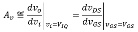
Page 372, Equation 7.13
The equation given is not the definition of
Av.
Change equation 7.13 to read as follows:
Page 475, Problem 7.5 part (c)
Replace the phrase, "and disregarding the distortion caused by the MOSFET's square-law characteristic," with the phrase, "and by using equations valid for large signals," . . .
The printed phrase is ambiguous. It has at least two equally valid interpretations. First, as the author intended, "disregard" meaning, "do not use a small-signal approximation to eliminate the distortion from the calculation, instead allow the distortion to be included in the calculation. Second, "disregard" meaning assume a linear approximation as if no distortion existed.Page 479, Problem 7.30.
(Posted 7/23/2020)
Replace the first sentence with: "Model the NMOS amplifier shown in Fig. P7.30 using a T equivalent circuit, assuming λ = 0."
("Replace the transistor. . ." misleads students into thinking that the DC sources, VDD and VSS play a part in the solution. In the needed small-signal analysis those DC sources get set to zero or ground.) (Posted 7/23/2020)Page 483, Problem D7.60 Part (a).
Change, "signal strength" to "signal voltage."
(Posted 7/23/2020)
Page 492, Problem 7.120.
Add the word "amplitude" to the last line of the problem statement so that it reads, ". . .provide 1-V amplitude pulses at the drain of Q2." Then add this sentence at the end of the problem statement:
"Assume the transistors have identical specifications."
Also see the additional note on this problem. (Posted 7/23/20, updated 1/23/2021)
Page 562, Problem 8.2.
The wording of this problem is ambiguous. To get the textbook's answers ignore the Early effect for transistor Q1 entirely. Apply the Early effect only to Q2 and then only when calculating ro and ΔIO. Even then there is one outright error in the given answers. The correct minimum output voltage using the above method is VO ≥ 0.14 V (not 0.2 V).
If the Early effect is taken onto account for both transistors, then the answers are: 68 kΩ, 6 μm, 0.125 V, 40 kΩ, and +5 μA.
(Posted 1/28/2021)
Page 562, Problem 8.4.
Insert a sentence before the word, "Neglect" so that the end of the problem statement reads as:
. . .
source is required to operate for V0 as high as 1.1 V. Choose
the ratio W/L to maximize the magnitude of the overdrive
voltage at the diode-connected transistor. Neglect channel-
length modulation.
(Posted 7/23/2020)
Page 565, Problem 8.28.
Add, "for both bias levels." to the last line of the problem statement so that the last line reads:
vo/vsig for both bias levels.
(Posted 7/23/20)
Page 572, Problem 8.77.
In the equation for Av change the "equals" sign (=) to an "approximately equal" (≈) sign. (Posted 7/23/20)
Page 665, Problem 9.72.
The wording of the problem statement in the textbook is ambiguous. The maximum ΔVt is the maximum difference one could find between the two transistor's threshold voltages when one transistor is compared to the other. Thus, the total maximum mismatch of threshold voltages is just 4 mV, say by making one 2 mV high and the other 2 mV low. However, the variabilities specified for the W/L ratios and for the RD resistors are specified "independently," meaning relative to their nominal values. Thus W1/L1 could be 1% high while at the same time W2/L2 could be 1% low, for a total mismatch of 2% The same applies to the drain resistances.
(Posted 2/27/2021)
Page 731, Figure 10.26 (a).
At the drain of QS (the blue text) change ZSS = RSS||CSS to ZSS = RSS||ZCSS
In the context of electronics the operator colloquially called "in parallel with" and denoted || should only be used with impedances.Page 771, Problem 10.50.
The operator || can be interpreted as a mathematical operator. To wit,
a||b = 1/[(1/a) + (1/b)]
In other words, || can mean, "take the reciprocal of the sum of the reciprocals." Given this interpretation, the expression RSS||CSS has a mis-match of units. Expressing this concept in terms of impedances is more correct.
The use of the || symbol as a mathematical operator, rather than simply as a substitute for the phrase, "in parallel with" is well entrenched in electrical engineering literature but is not formally standardized as far as Prof. dDB knows. This can lead to real confusion. For example, in the expression
Ceq = C1||C2 does this mean that the capacitors are, "in parallel" and thus the equivalent capacity is their sum, or does it mean that the capacitors are in series and the equivalent capacity is, "the reciprocal of the sum of the reciprocals?" This confusion can be avoided by using the parallel symbol, ||, only with impedances, e.g. Zeq = ZC1||ZC2. Then the symbol is helpfully meaningful no matter if it is interpreted as the phrase, "in parallel with" or as the mathematical operator meaning "reciprocal of the sum of reciprocals."
Reference: Wikipedia page on Parallel (operator)
(Posted 7/23/2020)
Replace the phrase "low-frequency gain" with the phrase
"mid-frequency gain."
It happens that the low-frequency transfer function, FL(s) = 1 in this instance.
Thus, FL(s)AM = AM, but since AM is what is wanted, that is what
should be requested.
(Posted 3/26/2021)
Appendix L, Page L-3, Answer to Problem 2.92.
The value given for C is wrong. The correct value is C = 39.8 pF.
(Posted 9/18/2020)
Appendix L, Page L-4, Answer to Problem 4.64.
There are errors of precision and other errors in the answers given.
Correct answers are:
(a) 9.825 V; (b) 205.6 Ω; (c) 3.293% of 10 V; (d) –6.770 Ω, –1.354% of 10 V; (e) 71.38 mA, 0.7370 W
(Posted 7/23/2020)
Appendix L, Page L-6, Answer to Problem 6.58.
There are rounding errors. Assuming |VBE| = 0.7 V, more accurate answers are +0.42 V, +1.12 V, –1.16 V; +1.2 V, +1.9 V, –1.9 V, 206
(Posted 7/23/2020)
Appendix L, Page L-6, Answer to Problem 6.63.
The answers given do not meet the specifications of the problem statement. With a little calculation it is clear that the emitter current will be out-of-specification for the β = 50 case. Correct answers are:
RB = 30 kΩ, RC = 4 kΩ, RE = 4 kΩ,
(0.919 mA) ≤ IC ≤ (1.004 mA) and (–1.33 V) ≤ VC ≤ (–0.903 V)
Hint: It is not sufficient to solve for the three resistor values and then round all three values. The emitter current is particularly sensitive to the value of RE. After that is rounded it will be necessary to recalculate RB to reset the emitter current back to 1 mA for the case of β = 100.
Note: A case might be made for adjusting RB as high as 39 kΩ. All specifications will then be met except that the emitter current for the case of β = 100 will be a bit low. (Posted 7/23/2020)
Appendix L, Page L-8, Answer to Problem 8.2.
The answers given assume that you will ignore the Early effect entirely for transistor Q1 and apply it to Q2 only when calculating ro and ΔIO. Even then thre is one outright error in the given answers. The correct minimum output voltage using the method described here is VO ≥ 0.14 V (not 0.2 V).
If the Early effect is taken onto account for both transistors, then the answers are: 68 kΩ, 6 μm, 0.125 V, 40 kΩ, and +5 μA.
(Posted 2/02/2021)
Appendix L, Page L-11, Answer to Problem 10.48.
The numerical answers given are poorly rounded. The conclusion in favor of the method of open-circuit time-constants is wrong. A correct answer is:
–143 V/V; 3.2 MHz; 2.47 MHz; The first estimate, from the
dominant pole approximation, is likely to be the best because a
loop of capacitors invalidates the accuracy of the method of
open-loop time-constants.
(Posted 3/26/2021)
Additional notes: (Clarifications--not errata)
Page 49 Problem 1.28
An equivalent problem (Implying the same questions and giving the same answer) is as follows:
Suppose a temperature sensor is at a temperature of T degrees centigrade. At this temperature and without the load resistance connected, an ideal voltmeter shows the output voltage to be V millivolts. A 10 kΩ load resistance is now connected but the temperature is not changed. The terminal voltage of the sensor is reduced to V – 10 mV. Now the temperature is increased until the terminal voltage returns to V millivolts. It is observed that the temperature was increased 20°C to accomplish this. What is the source resistance of the sensor?
(Posted 7/23/2020)
Page 122 Problem D2.36 part (b)
The output resistance of the "current amplifier" is requested. The variable vo designates the output of the "operational amplifier" which is not the output of the "current amplifier." The "current amplifier is the whole circuit except for the load resistance RL. The output of the "current amplifier" is the current, iL through the load resistor, RL.
Hint: In figure VE2.2 (page 71) add label VL under RL and polarity marks "+" and "–" on either side with the "+" on the left. Then the output of the "current amplifier" is the load current, iL = VL/RL.
To find the output resistance of the "current amplifier," replace RL by a test source, Vx such that VL = Vx. Then, with the input of the "current amplifier" zeroed (iI = 0 or open) find iL in terms of VL. Then the output resistance is Ro = VL/iL. See text page 30 for the basic theory. Note that for a current amplifier, a zero input is an open input. (Whereas, for a voltage amplifier a zero input is an input shorted to ground.)
Also see above for errata on Part (d). (Posted 7/23/2020)
Page 129. Problem 2.79 and Figure P2.79
The two resistors connected to the non-inverting ("+") inputs of the op-amps are for the purpose of reducing the non-ideal effects of input bias currents to the op-amps. The assumption of an "ideal" op-amp makes these resistors unimportant to the operation of the circuit, no matter what their values are (as long as the values are finite). If the op-amps are ideal these resistors may be set to zero (replaced with wires) without any change to the operation of the circuit. Additionally, although the two 10 kΩ resistors as shown will reduce the harmful non-ideal effects of input bias currents, these resistors are not shown with their optimal values. For this circuit, the non-inverting input of the top op-amp should be connected to node A through a 10 kΩ||10 kΩ = 5 kΩ resistor. The non-inverting input of the bottom op-amp should be connected to ground through a 10 kΩ||20 kΩ = 6.67 kΩ resistor. These are the Thevenin-equivalent resistances seen by the inverting inputs of the op-amps. If this makes no sense to you or you are further interested, ask professor De Boer about it.
(Posted 7/23/2020)
Page 131. Problem D**2.93
For stylistic consistency, in the denominator of the equation the second instance of j could be inside the parenthesis. The complete denominator is then
[1 + (ω1/jω)][1 + (jω/ω2)]
Either way, the equation means the same thing. (Posted 7/23/2020)Page 205–207 Example 4.7
In Figure 4.19, in both parts (a) and (b), VZ = VO.
Consequently, in part (b) of the figure. VZO ≠ VZ because VZO + rzIZ = VZ
In the statement of the example problem "VZ = 6.8 V at IZ = 5 mA" is given. This does not mean that the actual diode current, labeled in blue as "IZ" on the figure, is necessarily 5 mA. Nor does it mean that VZ (labeled in blue on the schematic as VO) necessarily equals 6.8 V. It only means that if IZ is 5 mA then VZ = VO will be 6.8 V.
(Posted 7/23/2020)
Page 240 Problem 4.76
Here is the question stated in one piece, with errata corrected:
4.76 Let the full-wave rectifier circuit shown in Figure 4.22 (page 211) operate from a 120 V (rms) 60 Hz residential supply line. Let the transformer have a 6:1 (step down) turns ratio. (The turns ratio from the primary to each half of the secondary is 12:1.) Let the diodes be silicon diodes that can be modeled to have a 0.7 V drop for any forward current. Let the load resistor be 500 Ω. Augment this rectifier circuit with a capacitor chosen to provide peak-to-peak ripple voltage of
(i) 10% of the peak output and
(ii) 1% of the peak output.
In each of the above cases:
a.) What average output voltage results?
b.) What fraction of the cycle does each diode conduct?
c.) What is the average current through each diode?
d.) What is the peak current through each diode?
Note: a "rectifier" is a diode or—in this case—a set of diodes used to convert alternating current to direct current.
Also see above for errata on this problem.
(The original problem statement refers to Problems 4.69 and 4.75. Problem 4.75 refers to Problem 4.68. Problem 4.68 refers by name—not by figure number—to Figure 4.21, but students are supposed to substitute Figure 4.22 because problem 4.69 refers to that by name and by way of superseding problem 4.68 because problem 4.76 mentions problem 4.69 instead of Problem 4.68. Even some professors have a hard time understanding the question as presented in the textbook!)
(Posted 7/23/2020)
Page 240 Problem 4.77
Here is the question stated in one piece, with errata corrected:
4.77 Let the full-wave bridge rectifier circuit shown in Figure 4.23 (page 213) operate from a 120 V (rms) 60 Hz residential supply line. Let the transformer have a 12:1 (step down) turns ratio. Let the diodes be silicon diodes that can be modeled to have a 0.7 V drop for any forward current. Let the load resistor be 500 Ω. Augment this rectifier circuit with a capacitor chosen to provide peak-to-peak ripple voltage of
(i) 10% of the peak output and
(ii) 1% of the peak output.
In each of the above cases:
a.) What average output voltage results?
b.) For what fraction of a cycle is there conduction through the secondary
winding of the transformer?
c.) What is the average current through each diode?
d.) What is the peak current through each diode?
Also see above for errata on this problem.
(The original problem statement refers to Problems 4.70 and 4.75. Problem 4.75 refers to Problem 4.68. Problem 4.68 refers by name—not by figure number—to Figure 4.21, but students are supposed to substitute Figure 4.23 because problem 4.69 refers to that by name and by way of superseding problem 4.68 because problem 4.77 mentions problem 4.70 instead of Problem 4.68. Even some professors have a hard time understanding the question as presented in the textbook!)
(7/23/2020)
Page 363, Problem D6.64.
The problem statement in the textbook is a little ambiguous.
Equivalent and less ambiguous language is as follows:
D 6.64 Consider the pnp transistor in the circuit of Fig. P6.64.
a.) If the transistor has β = 50, find the value for RC to obtain VC = +2 V.
b.) Using the value for RC found in part (a), what value of VC will
result if the transistor is replaced with one having β = 100?
(Posted 7/23/2020)
Page 492, Problem 7.120.
1.) When the problem refers to an "amplitude" it is referring to the absolute value of the quantity.
2.) The "50-
 coaxial cable" is
just a wire with a shield around it. Specifically, the
resistance from one end of the cable to the other is ZERO.
The resistance from the drain of Q1 to
the source of Q2 is 0 .
coaxial cable" is
just a wire with a shield around it. Specifically, the
resistance from one end of the cable to the other is ZERO.
The resistance from the drain of Q1 to
the source of Q2 is 0 . Further explanation
However, the cable is long enough so that it takes a noticeable amount of time for a signal to travel through the cable (or wire). Because of this propagation time, the cable works better when the load on the cable is of the specific value for which the cable is designed. This cable is designed for a 50 Ω load, thus it is called a "50-Ω coaxial cable," but just as for a wire, the resistance of the cable from end-to-end is (practically) zero. Thus the goal of the problem is to make Ri2, the resistance looking into the source of Q2, be 50 Ω so that the cable works as well as possible with respect to transferring high-bandwidth (fast) signals.
Videos related to this topic:
1.) Transmission Lines—Signal Transmission and Reflection
2.) Tektronix—Transmission Lines
3.) Transmission Line Terminations for Digital and RF signals
Also see errata on problem 7.120. (Posted 7/23/2020, updated 1/23/2021)
Page 569, Problem 8.55.
The wording of Part (b) of the problem statement in the textbook is a little confusing. This problem is asking for the transconductance, gm1 of transistor Q1 only, plus the output resistance of each of the transistors, ro1, ro2, and ro3. Equivalent and less ambiguous language is as follows:
b.) For transistor Q1 find the transconductance, gm1. For all three of
the transistors, find the associated output resistance due to Early
effect, ro1, ro2, and ro3 (Posted 2/03/2021)
Page 703, Section 10.3, The Method of Open-Circuit Time Constants
The presentation of this method is rather abbreviated in this textbook, which may lead students to erroneous conclusions. This method has some risks of producing bogus results if one is not careful to first confirm that the circuit satisfies the conditions of the theorem of Open-circuit Time Constants. Here is a statement of the theorem:
Each of the high-frequency poles of a circuit can be found exactly
if, in the small-signal model there are no inductors and any
capacitors in series or parallel are reduced to single equivalents
and there are no loops that involve only capacitors. And if one
prepares the circuit for open-circuit time-constant analysis by
taking these steps:
1.) Zero all signal sources.
2.) Open (set to zero farads) all the capacitors that
influence the high-frequency response.
3.) Short all other capacitors.
Then, for each of the capacitors, Ci that were opened, find the
Thevenin equivalent resistance Ri seen by each Ci and find the
associated pole frequency, ωi as the reciprocal of the product
(time constant), to wit. . .
ωi = 1/(RiCi)
After the pole frequencies are found from the open-circuit time-constant theorem one can then derive from them the denominator of the high-frequency transfer function, FH(s) and/or apply an approximation such as the dominant pole approximation (page 704) or the approximation shown on page 705 as Equation 10.63 to find the half-power frequency, ωH.
Furthermore, the approximation chosen is not part of the open-circuit time-constant method. The open-circuit time-constant method just gives a list of pole frequencies (or a list of time-constants). One is free to do as one pleases with that list. In addition to deriving the denominator of the high-frequency transfer function, or using a dominant pole approximation, or using equation 10.63, there is another approximation, not mentioned in the textbook, that can be used. This other approximation can be proven to be optimistic. However, it usually gives more accurate results than equation 10.63. (It always yields a result equal to or greater than the actual half-power frequency.) The approximation is:
The theorem of open-circuit time-constants and the various approximations that may be applied to the list of poles may be used even when the theorem's conditions do not exactly apply. However, one must be aware that if there are loops of capacitors then the open-circuit time-constant method will find more poles than actually exist! So, of course, the method cannot be exact in that case. Also, the method ignores any zeros that may exist. But if the extra pole(s) and or zero(s) is (are) not nearly dominant, then by coincidence the approximation of the half-power frequency can still be quite good.
(See for reference Grey and Searle, Electronic Principles: Physics, Models, and Circuits., Wiley, 1969, p531 and following.) (Posted 3/26/2021)
Page 891, Figure 12.3.
In the textbook's illustration, transistor Q3 is shown using the symbol for a diode. This is an industry shorthand. Actually, Transistor Q3 is identical to transistor Q2 except that it is diode-connected. Figure 12.3(expanded) shown below detials the way the three transistors shown in the textbook's Figure are actually connected.
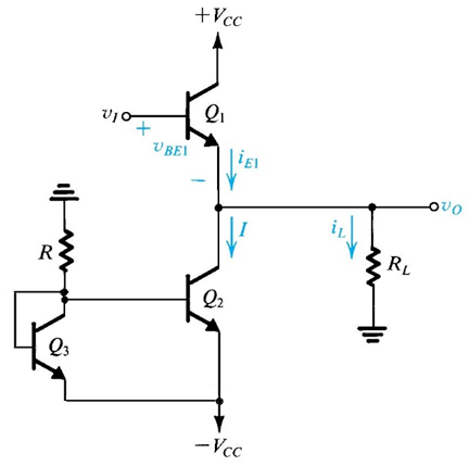
Figure 12.1(expanded) An emitter follower (Q1) biased
with a constant current I supplied by current mirror Q2-Q3.
(Posted 4/20/2021)
Appendix G, page G-18, Problem G.9
For the BJT transistor assume
 is infinite.
 For both the MOSFET and the BJT ignore the Early effect.
(Posted 7/23/2020)
Disclaimer: This list of errata is provided by Professor De Boer for the use of his students in his courses. Professor De Boer has no connection to the book's publisher or the authors of the textbook. This list is offered as is, with no guarantee of any kind. It is likely to be incomplete at the least. Anyone may suggest newly discovered errata for inclusion in this list. Send suggestions by e-mail to Douglas.DeBoer@Dordt.edu