Professor De Boer's list of
TEXTBOOK ERRATA
(last update 2/05/2011)
Sedra & Smith,
Microelectronic Circuits, 5th Ed.
ISBN 0-19-514251-9, Oxford, 2004.
Link to errata for the 6th edition, 7th edition, 8th edition.
If you are considering purchasing this textbook and worrying that
it is a poor choice due to the length of this list of errata, please
reconsider. Competing textbooks have about as many errata, but perhaps
no list like this. "Better the devil you know than the devil you don't."
Professor
De Boer likes this book enough to find it worthwhile
to publish this list of errata.
Page 51,
Two lines above the heading RESISTORS AND OHM'S
LAW Replace "Appendix D" with "Appendix C."
Page 127, Problem D2.33 part (c)
Add the word "Norton" between "a" and "current". Also add,
"Assume ideal operation without saturation." to the end of the
problem statement for part c.
Page 229, Problem 3.83
In part (c) add the phrase, "during conduction." The question
then reads. . .
c.) What is the average diode current during conduction?
(Posted 10/21/2008)
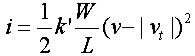
Page 361, Problem 4.18, part (a)
Insert "(1/2)" between the equals sign and the k'. The
equation should be:
Pge 365, Problem 4.46.
In the first line of the problem statement delete the space
between the number 2.5 and the "µp".
Also, put the number in parenthesis. The first line then ends
with this expression:
µnCox = (2.5)µpCox =
Better: just specify directly what is intended:µnCox = 20 µA/V2,
µpCox = 8 µA/V2
(As printed µnCox = 2.5 µA/V is a correct reading but that was not the author's intention.)
Page 366, Problem 4.49 part (c)
Replace the phrase, "and disregarding the distortion caused by the MOSFET's square-law characteristic," with the phrase, "and by using equations valid for large signals," . . .
(The printed phrase is ambiguous. It has at least two equally valid interpretations. First, as the author intended, "disregard" meaning, "do not use a small-signal approximation to eliminate the distortion from the calculation, instead allow the distortion to be included in the calculation. Second, "disregard" meaning assume a linear approximation as if no distortion existed.)
Page 369, Problem 4.74.
Replace the first sentence with: "Model the NMOS amplifier shown in Fig. P4.74 using the T equivalent model shown in Fig. 4.39(d)."
("Replace the transistor. . ." misleads students into thinking that the DC sources, VDD and VSS play a part in the solution. In the needed small-signal analysis those DC sources get set to zero or ground.)
Page 371, Problem 4.86.
Add this sentence to the problem statement:
"Assume the transistors have identical specifications."
(posted 10/31/06)
Page 517, Problem 5.1.
For case 8, in the column labeled "B," change "5.0" to "–0.5."
(posted 12/05/08)
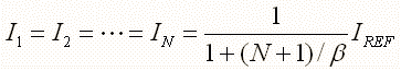
Page 571, Exercise 6.8,
The right-hand side of the equation should be multiplied by IREF. The correct equation is:
Page 589, Figure 6.21
Near the dependent current source, replace gmR'L with gmVgs
(posted 2/26/07)
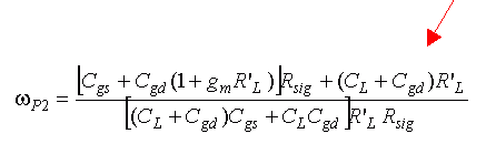
Page 593, Equation 6.67.
In some printings of the text the instance of Cgd pointed out below by the red arrow is incorrectly shown as Cgs. The illustration below gives the correct equation. (updated 2/25/2009)
Page 598, Equation 6.80
In the denominator delete R'L. (posted 3/05/07)
Page 631, Equation 6.145
Delete the negative sign.
(Avo is a negative number. An additional negative sign is incorrect.)
(posted 3/28/07)
Page 672, Problem 6.57.
Change part (a) so that it reads as follows:
(a) Neglecting the DC current in the feedback network and the effect of ro,
find VGS. Then find the DC current in the feedback network and VDS. Verify that you were justified in neglecting the current in the feedback network when you found VGS.
(Note: Given the original wording, some students assume there is no DC current in the bias network since it can be neglected at first. Then they find
VDS = VGS but this is incorrect. A quantity that can be neglected in one particular analysis is not necessarily zero.)
Page 677, Problem 6.94.
Change part (b) by adding "
 = ∞" to the list of given values. Then the second line
of part (b) will read: "for the case = ∞, Cπ =
14 pF, . . ."
(posted 2/16/09)
= ∞" to the list of given values. Then the second line
of part (b) will read: "for the case = ∞, Cπ =
14 pF, . . ."
(posted 2/16/09)
Page 775-776, Problem 7.10.
Change "vid = vG2 – vG1" to "vid = vG1 – vG2"
(The above correction makes the problem consistent with Eq. 7.15, the discussion associated with Fig. 7.5, and the answer posted in the back of the textbook.)
Also note that in one place the problem statement mentions "iD2/iD1" and in another place it is "iD1/iD2". That is not errata (but it could be confusing).
(posted 4/11/2007)
Page 777, Problem D7.24.
Change "let the BJT
be very
large:"
to "let the BJT
= 100:"
(Part d requires that
=
100, so the formulae developed in parts a-c should include
finite . Also note that the
answer in the back of the book is wrong. See Page H-4, Answer to Problem D7-24 below.)
Page 797, Top third of the page
The discussion of signal-to-noise ratio presented (as printed) is in terms of a voltage ratio. This is not a common practice in the industry. Usually the signal-to-noise ratio is defined as a power ratio. The following changes make the text conform to industry standard practice.
In the first line on the page add the word "power" so that it reads, "signal-to-noise power ratio for this amplifier is"
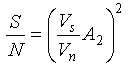
Change Equation 8.13 to S/N = Vs2/Vn2
In the line below Equation 8.14 change, "signal-to-noise ratio" to, "signal-to-noise power ratio".
Change Equation 8.15 to
In the line below Equation 8.15 change, "which is A2 times higher" to,
"which is A22 times higher".
References:Page H-1, Answer to Problem 1.9.
—The definition of signal-to-noise ratio as a power ratio (not a voltage ratio) can be found in most handbooks of electrical engineering.
—Pallas-Areny and Webster, Analog Signal Processing, Wiley-Interscience, 1999, page 16 and pages 525-526.
—Millman and Halkias, Integrated Electronics: Analog and Digital Circuits and Systems, McGraw Hill, 1972, p403.
—Wikipedia, "Signal-to-noise ratio"
(Posted 4/09/2009)
Change the second instance of "157" to "106". Also fix the grammar: Just before the first instance of "a 157" add the word "with".
Page H-2, Answer to Problem 3.9 part b
The answer should be "–1.67 V; 0 A." (A minus sign is missing in the text.)
Page H-2, Answer to Problem 3.10 part b
Change "2 V" to "–2 V" (A minus sign is missing in the text.) (posted 3/29/07)
Page H-2, Answer to Problem 3.78.
Change "94.7%" to "47.4%."
(Alternatively, change the question. Specifically change, "For what fraction of a cycle does each diode conduct?" to, "For what fraction of a cycle is there conduction through the load?" Answer: 94.7%)
Page H-2, Answers to Problem 3.114
The answers shown in the text are wrong. The correct answers are:
691 mV; 424 nm; 212 nm (each side of the junction); 33.9 fC; 24.5 fF
(posted 9/22/08, updated 9/23/08)
Page H-2, Answers to Problem 4.34
Answers given are wrong. The correct answers are RD = 2.5 K
 ,
RS = 500 .
,
RS = 500 .
(Alternatively, to find the answers given in the text, change "2.5 V" to "5 V" in two places on Fig. 4.20.)
Page H-2, Answer to Problem 4.46 (b) is inaccurate.
Change "4.8 μA" "to 4.5 μA". Students should express answers to part (b) that are accurate to at least 3 significant figures—one more than given in this answer key.
Page H-2, Answers to Problem 4.65 are inaccurate.
Correct answers are: 36 k
,
195 μA, 1.99 V.(Increasing RD cannot increase the current!)
Page H-3, Answer to Problem 5.1
This answer may appear to be wrong, but it is correct.
There is errata in the problem statement.
(updated 12/05/2008)
Page H-3, Answer to Problem 5.20 part (d)
Change "0.35 V" to "–4.475 V"
Page H-3, Answer to Problem 5.67 part (b)
Change "1.8 mA, 0.3 mA" to "0.2 mA; 2.3 mA"
Page H-3, Answer to Problem 5.124
Change "0.63 V/V" to "–0.63 V/V" (posted 01/29/07)
Page H-3, Answer to Problem 5.168
Change "19" to "11" (or the design can be pushed to "12" with only a very slight compromise in the noise margin.) (posted 02/06/07, updated 02/13/07)
Page H-3, Answer to Problem 6.59
Change "1.4 V" to "1.07 V" (posted 02/05/2011)
Page H-3, Answer to Problem 6.108
Change "0.45 V/V" to "0.63 V/V" (posted 02/06/07)
Page H-4, Answer to Problem D7-10
Answers to the quesitons, "What is the differential voltage, vid = vG1 – vG2, for which the ratio of drain currents iD2/iD1 is 1.0? 0.5? 0.9? 0.99?" are not given.
(posted 4/26/2007)
Page H-4, Answer to Problem D7-24
Change "(I/2)" to "(αI/2)" in each instance of parts a and b.
In part c change "4 V" to "4.04 V"
In part d change "0.4 mA, 10 k
" to 0.404 mA, "10 k." (updated 4/17/2007)
Page H-4, Answer to Problem 7-37
Change "40 V/V; 50 k
" to
"33.0 V/V; 60.6 k."
Additional notes: (Clarifications--not errata)
Page 133. Problem 2.77 and Figure P2.77. (added 9/19/08)
The two resistors connected to the non-inverting ("+") inputs of the op-amps are not the optimal values. For this circuit, the non-inverting input of the top op-amp should be connected to node A through a 6.67 k
resistor. The
non-inverting input of the bottom op-amp should be connected to
ground through a 7.5 k resistor.
These assumption of an "ideal" op-amp makes these resistors
unimportant to the operation of the circuit, no matter what their
values are. If the op-amps are not ideal, these two resistors
reduce the effect of input bias currents. If this makes no sense
to you and you are further interested, ask professor De Boer about
it.
Page 138. Problem D**2.126. (added 9/26/06)
For stylistic consistency, in the denominator of the equation the second instance of j could be inside the parenthesis. The complete denominator is then
[1 + (w1/jw)][1 + (jw/w2)]
Either way, the equation means the same thing.Page 169 Example 3.8
In the statement of the example problem VZ = 6.8 V at IZ = 5 mA is given. This does not mean that the actual diode current, labeled in blue as "IZ" on the figure, is necessarily 5 mA. It only means that if IZ is 5 mA then VZ (and in the figure, VO) will be 6.8 V.
Page 229 Problem 3.85
Here is the question stated in one piece:
3.85 Augment the rectifier circuit shown in Figure 3.27 (page 176) with a capacitor chosen to provide peak-to-peak ripple voltage of (i) 10% of the peak output and (ii) 1% of the peak output. In each case:
a.) What average output voltage results?
b.) What fraction of a cycle is there conduction through the bridge of diodes?
c.) What is the average current in each diode during conduction?
d.) What is the peak diode current for each diode?
(The original problem statement refers to problems 3.83 and 3.78. Problem 3.83 refers to Problem 3.76. Problem 3.78 refers by name (not by figure number) to Figure 3.27. Students have a hard time understanding the question.) Posted 10/21/2008.
Page 370, Problem 4.78.
The main part of the problem is a proof ("Show that this tangent. . ."). A sketch is requested to illustrate the proof. An initial sketch might be easier if you assume numerical values for the transistor's parameters, but keep the proof and the final sketch generic (no specific numbers on the axes for example). On the final sketch, label important features such as the operating point and label the axes appropriately. (posted 10/21/2008)
Page 667, Problem 6.9.
For the BJT transistor assume
is infinite. For both the MOSFET and the BJT
ignore the Early effect.
(posted 01/31/07)
Page 805, Figure 8.10.
In parts b and c of the figure, the circuit element h22 has units of conductance (siemens). The actual resistance is (1/h22)
. This is not a miss-print since
conductors and resistors share the same symbol.
Disclaimer: This list of errata is provided by Professor De Boer for the use of his students in his courses. Professor De Boer has no connection to the book's publisher or the authors of the textbook. This list is offered as is, with no guarantee of any kind. It is likely to be incomplete at the least.