#


(In Mano & Kime unless otherwise noted)
---
---
After peer grading we will review for the exam.
5/02
at
5 PM
5/03#
at
7 PM
zoned recording and logical block addressing.
Do 12-1*, 12-3, And answer this question:
12-A What are the advantages of packet-based
I/O such as in USB?
Note errata on page 601.
Note errata on problem 12-1*.
This assignment will be due for regular grading
a 5 PM on Friday. Place your homework in a box
that will be placed near Prof. De Boer's office
door. The box will be labeled "EGR 204
Homework." This assignment will be graded and
placed in the plastic bin for "De Boer's
Courses" by noon on Saturday. You may then
pick up your homework at your convenience on
Saturday afternoon.
5/02
5/03#
at
7 PM
Do 10-27*, 10-29
Note errata on problem 10-27*.
This assignment will be graded and placed in
the plastic bin labeled "De Boer's Courses" by
noon on Saturday. You may pick up your
homework at your convenience on Saturday
Afternoon.
Please bring a #2 pencil (or a mechanical
pencil with HB lead) to class on Wednesday.
Before the end of class we will fill in
course evaluation forms. (I.D.E.A. forms.)
4/30
5/02#
Do 10-23*, 10-24, 10-25*
Hint: For Problem 10-23* assume that the
"16" bit register is named "R".
Hint: For Problem 10-25* a computer does
subtraction A - B as A + (-B) and assumes the
numbers are twos complement signed integers.
Then "borrow" is the NOT of the carry out of
that addition. This borrow is saved in the
carry flag bit in place of the normal carry bit.
4/28
4/30#
Do 10-18, 10-20*, 10-21
Note: On 10-18 work the problem in base ten
using 13 places right of the radix point.
Note: On 10-20* the answer posted on the web
is wrong. The meaning of E is incorrect on the
first and last lines. You should list all the
binary bit patterns possible (e in binary) and
the value of the exponent (E in decimal) in
a style similar to the outer two columns of
Table 10-6 on page 526. Also note carefully
the text underneath Table 10-6.
Note: On 10-21 for part (b) list
E = (the smallest), -1, 0, 1, and (the largest)
values possible. On part (c) the calcuation
should be an estimate in base ten and in
scientific notation, to at least three significant
figures of the largest and smallest positive
normalized numbers.
4/25
4/28#
Do 10-3*, 10-4, 10-17*
4/23
4/25#
Do 10-5, 10-6*, 10-7
4/21
4/23#
Do 10-1, 10-2*
Hint: You might find it easier to work on
10-2* first.
For both 10-1 and 10-2*,
SUB and DIV are not described in the text.
Some examples are shown below:
Three Address Instructions:
SUB R1, R2, R3 R1
DIV R1, R2, R3 R1
Two Address Instructions:
SUB T1, T2 M[T1]
DIV T1, T2 M[T1]
One Address Instructions:
SUB X ACC
DIV X ACC
Hint for 10-2: Part (b) requires only two
temporary memory variables.
4/18
4/21#
Do 9-12, 9-15
Hints for problem 9-15:
It might be easier to do part (b) first.
For part (a) fill unused fields with "X" for
"don't care." Note that address fields are the
only kind that can be unused since Figure 9-6
shows explicit logic for the other fields.
For part (a), line 3, in "R[5] + 2" the "2" arrives
from the "Constant in" lines to MUX B. (See
Figure 9-15 on page 471.)
In part (a) line 5 the "PC + se PC" should be
"PC + se AD". Also let AD = 25 (base ten--
convert it to binary). The value of AD is supplied
in a pair of fields, split to "Left" and "Right." The
left is most significant. This forms effectively a
six-bit field. (See Figure 9-14 on page 467.)
Note errata on problem 9-15.
4/16
4/18#
Do 9-8*, 9-9
Hints on problem 9-9:
Zero can be formed as the exclusive OR of two
identical words. For example, R0 XOR R0 = 0.
Assume numbers are signed integers in the twos
complement number system. Then
                    _
        X - Y = X + Y + 1
It is possible that some bits in the control
word do not matter. Mark those as "X" for
"Don't Care"
Although 9-10* is not assigned, understanding
that problem and its solution (posted on the
web) might help you understand and do 9-9.
4/14
4/16#
Do 9-1, 9-2*
Note: In 9-1, "selection lines" refers to
"Destination Select," "A Select," and "B Select"
Note: For problem 9-2* assume the ALU is
designed to work with numbers in twos
complement format. Overflow detection is
described on page 165 of your text. The result
of your logic should be that N = 1 iff the
output of the ALU represents a negative number.
Bit Z = 1 iff the output represents zero.
Bit V = 1 iff there was an overflow.
Bit C = 1 iff there was a carry out of
the most significant place.
4/11
4/14#
Do 8-9, 8-10, 8-11
Note: From 3/31 through 5:55 pm on 4/07 the
last problem was shown incorrectly as "1-11"
instead of 8-11.
4/09
4/11#
Do 8-7, 8.8*
Note errata on problems 8-7 and 8-8 .
4/07
4/09#
Do 8-1*, 8-2, 8-3* EXCEPT change
"64K X 16" to "1 M x 4" and change
"32000" to "196865." Note: The solution
given online goes with the problem as printed
in the textbook. The assignment is to re-work
the problem with the organization and address
given here.
4/04
4/07#
Do 7-11* Note errata on p404, Problem 7-11*
Note Figure 7-15 too.
7-16 and use hierarcy including a diagram of a
single cell of the register.
4/02
4/04#
page 353 through the end of the Section.
Do 7-4*, 7-5*, 7-8
3/31
4/02#
on page 353.
Do 7-3, 7-B
3/28
3/31#
Do 7-A (click on link), 7-2*
Here is a datasheet for the '175 (problem 7-A).
See especilly the function table on page 3 and
the block diagram on the right side of page 3.
---
---
Study for Test on Wednesday, 3/12.
3/26
3/28#
Do 6-9. Answers should be in the style of. . .
"Signal RX at X ns has a <name problem>."
Hint: The times mentioned in the answers always
correspond to a clock edge.
6-15 and also specify how to connect the inputs
X, Y, and Z to the ROM and how to connect the
outputs A, B,C, and D to the ROM.
(Note errata on 6-15),
6-20 except mark fuses to remain intact on the
fuse map for a TIBPAL16L8-25C part. The fuse
map can be found on page 5 of the datasheet.
Hint 1) The output pins of the TIBPAL16L8-25C
are driven by inverters. You need to build the
complementary function into the array in order
to get correct outputs at the pins.
Hint 2) If you put an "X" mark on an AND gate
it signifies that all the fuses on all the
inputs for that AND gate should remain intact.
This forces the output of that AND gate to be
logic-0 always.
Hint 3) Tie pin 1 to ground. Use that input to
enable outputs.
3/10
3/12#
Do 5-35 using this state assignment:
A = 00, B = 01, C = 10, D = 11
Note that the problem statement continues on
page 291 underneath Figure 5-45.
Note errata on page 251.
Note errata on pages 254, and 259.
3/07
3/10#
Read Ch 5 Sec 5-5 from page 240 to the end.
Do 5-12, 5-13*
Note errata on page 243.
Note: Discussion of Problem 5-12
3/05
3/10#
"Designing With D Flip-Flops" on page 240.
Do 5-9, 5-11*
3/03
3/05#
Do these problems:
5-A. Draw a gate-level logic diagram of the SR
master-slave flip-flop shown in Figure 5-9 on
page 216. (Note Figure 5-7 on page 213.)
5-B. (Click on the link.)
5-6 (On page 281 in your text.)
2/29
3/03#
Do 5-4
2/27
2/29#
Do 5-1, 5-2.
Note: For these problems use the input
sequences given in the tables below. Fill in
the outputs shown on these tables. The
complete table or the equivalent information
in a vector waveform file print-out is the
answer.
  _  _      _                      _
  S  R | Q  Q         C  S  R | Q  Q
  -----+-----         --------+-----
  1  1 |              0  0  0 |
  1  0 |              0  0  1 |
  0  1 |              0  1  0 |
  1  1 |              0  1  1 |
  0  1 |              1  0  1 |
  0  0 |              1  0  0 |
  0  1 |              1  1  0 |
                      1  0  0 |
  Table for 5-1       1  1  0 |
                      1  1  1 |
                      1  1  0 |
                      1  1  1 |
                      1  0  0 |

                      Table for 5-2
Optional supplemental reading: RS Nand Latches.
2/25
2/27#
Do 4-23
Hint: Although 4-20* is not assigned, look at
that problem statement and its solution which
is posted on the web.
Another Hint: The sentence, "Note that
complemented inputs are available." means that
although the signal a_n is a separate input
from a, you should assume that a_n is always
the logical not of a. Wherever you might like
to use
 you
should instead use the signal a_n.
you
should instead use the signal a_n. The same goes for the other similarly named
pairs of signals.
2/22
2/25#
Do 4-4 except do it in this order:
1.) The given numbers are unsigned binary.
Pad each with leading zeros until it is
eight bits wide. This converts the
numbers from unsigned binary to signed
two's complement (and all of them are
positive).
2.) Negate subtrahends by taking the
two's complement.
3.) Add. The result is the answer without
any further manipulation. The answer is
in the two's complement notation.
4.) For each case, note if there is
"overflow" or "no overflow."
4-45 Note: this problem is not in the
textbook, click the link to view it.
2/20
2/22#
Do 4-2* (Use manual verification),
4-3* except assume the given numbers are
signed and in the 1's or 2's complement system.
By "obtain[ing]" the complement it is intended
that you negate the given number.
Also for each note if there is overflow or not.
Definition: Overflow upon negation occurs iff
negating a non-zero number does not change the
sign of the number. Note: the given unsigned
numbers are positive by definition, regardless
of the most significant bit (there is no sign
bit.) Thus, negating a number by complementing
it should result in a number with a sign bit
equal to logic-1. (If not, then overflow.)
In the above definiton, the phrase, "non-zero"
was inserted on Monday, 2/18, at 10:12 AM.
Note errata on Page 166
(Above note on errata was added 2/18 at 3:31 pm)
2/18
2/20#
Do 4-1 except begin with a truth table, then
use K-maps to derive equations for outputs
C2, S1, and S0. Stop with equations in SOP form
since drawing a schematic will be too tedious.
Note that the inputs are A1, A0, B1, B0, and C0.
You will need five-variable K-maps for this
problem.
----
----
Study for the Test on Wednesday, 2/13.
2/15
2/18#
Do 3-42*, 3-46, 3-47*
2/11
2/15#
Do 3-21,
3-32 except use a type '138 decoder and NAND
(instead of OR) gates.
Hint 1) Output a logic-1 to a LED to turn it on.
Hint 2) Read part (b) before doing part (a).
Hint 3) Use a block symbol for the '138
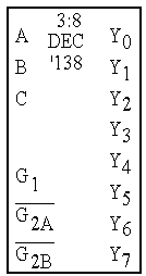
decoder rather than drawing all the gates.
This decoder is comparable in function to the
the one shown in your text in Figure 3-33.
Hint 4) Use value fixing on unneeded gate inputs.
Note: Professor De Boer assigned this problem
because it poses an interesting technical
challenge, but he does not endorse gambling.
3-35*
Note errata on Figure 3.33
2/08
2/11#
Do 3-20, 3-24, 3-25
2/06
2/08#
Do 3-1, 3-2*, 3-16
2/04
2/06#
Do 2-8, 2-30, 2-34
2/01
2/04#
Do 2-24, 2-25*, 2-31
1/30
2/01#
Do 2-15*, 2-16, 2-19*
1/28
1/30#
Do 2-7*, 2-11, 2-12*, 2-14
Note errata on problem 2-12*
Note errata on page 60, Figure 2-9(b)
Note on 2-14: "Optimize" means to "simplify"
as shown by several examples in section 2-4.
1/25
1/28#
Do 2-1*, 2-2*, 2-10*
1/23
1/25#
Do 1-10*, 1-22, 1-24, 1-25*
1/21
1/23#
Do 1-4, 1-5, 1-6, 1-7*, 1-8, 1-9*
Note: The answer to 1-5 must be exact.